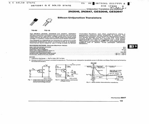
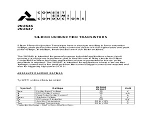
2N2646, 2N2647, GES2646, GES2647 Silicon Unijunction Transistors TO-92 TO-18 The GE/RCA 2N2646, GES2646 and 2N2647, GES2647 silicon-unijunction transistors have an entirely new structure resulting in lower saturation voltage, peak-point current and valley current as well as a much higher base-one peak pulse voltage. In addition, these devices are much faster switches. The 2N2646 and GES2646 are intended for general purpose industrial applications where circuit economy is of primary importance, and is ideal for use in firing circuits for Silicon MAXIMUM RATINGS, Abso/ute-Maximum Values: EMITTER REVERSE VOLTAGE ..........0 cee e cece ence ener eens INTERBASE VOLTAGE ........ ccc cece cece cece eee teen eens PEAK EMITTER CURRENT (Note 1) POWER DISSIPATION (NOt6 2)... 0... cece ccs euee ees eeaeeeees OPERATING TEMPERATURERANGE...........0..0ceceseenes Controlled Rectifiers and other applications where a guaranteed minimum pulse amplitude is required. The 2N2647 and GES2647 a
 5 Pages, 344 KB, Scan
2N2646, 2N2647, GES2646, GES2647 Silicon Unijunction Transistors TO-92 TO-18 The GE/RCA 2N2646, GES2646 and 2N2647, GES2647 silicon-unijunction transistors have an entirely new structure resulting in lower saturation voltage, peak-point current and valley current as well as a much higher base-one peak pulse voltage. In addition, these devices are much faster switches. The 2N2646 and GES2646 are intended for general purpose industrial applications where circuit economy is of primary importance, and is ideal for use in firing clrcuits for Silicon MAXIMUM RATINGS, Absolute-Maximum Values: EMITTER REVERSE VOLTAGE INTERBASE VOLTAGE ............. AMS EMITTERCURRENT........... PEAK EMITTER CURRENT (Note 1) POWER DISSIPATION (Note2)........ OPERATING TEMPERATURE RANGE..............-.- STORAGE TEMPERATURERANGE...............000000. 00sec NOTES: 1. Capacitor discharge 10uF or less, 30 V or less. Controlled Rectifiers and other applications where a guaranteed minimum pulse amplitud
 5 Pages, 184 KB, Scan
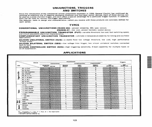
ach can be used for various non-trigger applications. The featuresboth in design and characteristicswhich you receive with these products are concisely defined for each series: TYPES CONVENTIONAL UNIJUNCTIONS 2N489-494proved reliability; MIL spec version. 2N2646-47low cost, proved hermetic sealed device. PROGRAMMABLE UNIJUNCTION TRANSISTOR (PUT)variable threshold, low cost, fast switching speed, and circuit adjustable electrical characteristics. COMPLEMENTARY UNIJUNCTION TRANSISTORu!timate in temperature stability for timing and oscillator applications. SILICON UNILATERAL SWITCH (SUS)-a stable fixed low voltage threshold, low cost, high performance 4-layer diode. SILICON BILATERAL SWITCH (SBS)low voltage triac trigger, two silicon unilateral switches connected back to back. SILICON CONTROLLED SWITCH (SCS)high triggering sensitivity, 4-lead capability for multiple loads or dv/dt suppression. APPLICATIONS Unijunctions . Device Triggers Conventional Complementary Programmable 2N489-94, 2N2646<
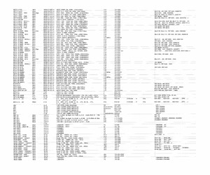
 6 Pages, 1753 KB, Scan
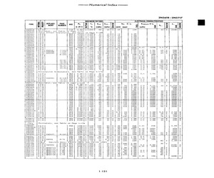
 30 4.3 2N2421 390 6.8 0.75 8.0 20 12 @ 60 5.0 2N2421A 390 6.8 0.75 8.0 20 12 @ 60 4.6 2N2421B 300 6.8 4.7 -6.8 8.0 6.0 0.2 @ 30 4,6 2N2422 390 9.1 0.75 8.0 20 12 @ 60 5.0 2N2422A 390 9.1 0.75 8.0 20 12 @ 60 4,6 2N2422B 300 9.1 0.62 -0.75 8.0 6.0 0.2 @ 30 2N2646 4-70 300 4.7 (min) 0.56 4.0 25 12 @ 30 2.0 2N2647 4-70 300 4.7 (min) 0.68 8.0 2.0 0.2 @ 30 2.0 2N2840 300 4.7 -9.1 1.3 -1.5 0.70 10 1.0 @ 30 2N3406 450 8.0 2N3479 400 4,7 -9.1 0,47 -0.62 6.0 20 12 @ 30 5.0 2N3480 400 9.1 0.75 4.0 15 12 @ 30 5.0 2N3481 400 9.1 0.85 6.0 15 12 @ 30 5.0 2N3482 400 4.7 -6.8 0.51 -0.62 8.0 2.0 0.02 G@ 30 5.0 2N3483 400 9.1 0.72 8.0 2.0 1.0 @ 30 5.0 2N34 84 400 9.1 0.85 8.0 2.0 0.2 @ 30 5.0 2N3679 250 9.1 0.80 4.2 2N3980 4-72 360 8.0 2N4851L 4-74 300 4.7 (min) 0.56 (min) 2.0 2.0 0.1 @ 30 2.5 2N4852 4-74 300 4.7 (min) 0.70 (min) 4.0 2.0 0.1 @ 30 2.5 2N4853 4-74 300 4.7 (min) 0.70 (min) 6.0 0.4 0.05 @ 30 2.5 2N4870 4-78 300 4.0 (min) 0.56 (min) 2.0 5.0 0.05 @ 30 2.5 2N4871 4-78 300 4.0 (min) 0.70 (min) 4.0 5.0 0.0
 5 Pages, 220 KB, Scan
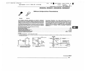
2N2646 2N2647 SILICON UNIJONCTION TRANSISTORS Silicon Planar Unijunction Transistors have a structure resulting in lower saturation voltage, peak-point current and valley current as well as a much higher base-one peak pulse voltage. In addition, these devices are much faster switches. The 2N2646 is intended for general purpose industrial applications where circuit economy is of primary importance, and is ideal for use in firing circuits for Silicon Controlled Rectifiers and other applications where a guaranteed minimum pulse amplitude is required. The 2N2647 is intended for applications where a low emitter leakage current and a low peak point emitter current (trigger current) are required and also for triggering high power SCR's. CASE MAXIMUM RATINGS (*) TJ=125C unless otherwise noted Symbol Ratings 2N2646 2N2647 VB1E Base 1 - Emitter Voltage 30 V VB2E Base 2 - Emitter Voltage 30 V IFRMS RMS Emitter Current 50 mA IEM Emitter Peak Current 2 A PTOT Total Power Dissipation
 2 Pages, 54 KB, Original
 BOX 5012 + DALLA! MENTS $, TEXAS 75222TYPE NUMBER INDEX TYPE NO. 2N2394 2N2395 2N2396 2N2432 2N2432A 2N2453 2N2483 2N2484 2N2497 2N2498 2N2499 2N2500 2N2537 2N2538 2N2539 2N2540 2N2586 2N2604 2N2605 2N2608 2N2609 2N2639 2N2640 2N2641 2N2642 2N2643 2N2644 2N2646 2N2647 2N2802 2N2803 2N2804 2N2805 2N2806 2N2807 2N2880 2N2894 2N2904 2N2904A 2N2905 2N2905A 2N2906 2N2906A 2N2907 2N2907A 2N2913 2N2914 2N2915 2N2915A 2N2916 POWE RRefer to The Power Semiconductor Data Book for Design Engineers, First Edition (CC-404). SEC.-PAGE 4-121 4-123 4-123 4-125 4-125 4-127 4-129 4-129 4-131 4-131 4-131 4-131 4-132 4-132 4-132 4-132 4-136 4-138 4-138 4-142 4-142 4-143 4-143 4-143 4-143 4-143 4-143 4-145 4-145 4-147 4-147 4-147 4-147 4-147 4-147 POWER 4-149 4-151 4-151 4-151 4-151 4-151 4-151 4-151 4-151 4-163 4-163 4-163 4-163 4-163 TYPE NO. 2N2916A 2N2917 2N2918 2N2919 2N2919A 2N2920 2N2920A 2N2944 2N2944A 2N2945 2N2945A 2N2946 2N2946A 2N2972 2N2973 2N2974 2N2975 2N2976 2N2977 2N2978 2N2979 2N2987 2N2988 2N2989 2
 1236 Pages, 34058 KB, Scan
2N2646 Spec Sheets Details Diodes, Transistors, Thyristors, Triacs, Dio... 1 of 2 http://www.americanmicrosemi.com/information/spec/?ss_pn=2N2646 HOME | CATALOG | CART |EXPRESS CHECKOUT | PARTS WATCH | NEW ITEMS |RFQ| Home 2N2646 Availability Online Store Diodes Buy 2N2646 at our online store! Transistors Integrated Circuits Special Offers: FREE UPS Ground Shipping on Orders above $150.00 Lanuage Translator: 2N2646 Information Optoelectronics Did you Know... Thyristors Category Thyristors Products Not only is AMS a leading Class Unijunction Transistors electronics distributor, we Search for Parts Type PN (N-Type Base) Request a Quote Test Houses parts to your exacting 2N2646 Specifications Information Spec Sheets Military/High-Rel : N Testimonials Store Policies Contact Us are being launched all the time. Give us a call to find Absolute Max. Power Diss. (W) : 300m FAQs Company specifications? New AMS semiconductor product lines Tuto
 2 Pages, 264 KB, Original
2N2646 2N2647 SILICON UNIJUNCTION TRANSISTORS Silicon Planar Unijunction Transistors have a structure resulting in lower saturation voltage, peak-point current and valley current as zell as a much higher base-one peak pulse voltage. In addition, these devices are much faster switches. The 2N2646 is intended for general purpose industrial applications where circuit economy is of primary importance, and is ideal for use in firing circuits for Silicon Controlled Rectifiers and other applications where a guaranteed minimum pulse amplitude is required. The 2N2647 is intended for applications where a low emitter leakage current and a low peak point emitter current (trigger current) are required and also for triggering high power SCR's. ABSOLUTE MAXIMUM RATINGS Tj=125C unless otherwise noted Symbol VB2E Ie ie VB2B1 PD TJ TStg Ratings Emitter-Base2 Voltage RMS Emitter Current Peak Pulse Emitter Current * Interbase Voltage RMS power Dissipation Junction Temperature Storage Temperature Capacit
 3 Pages, 96 KB, Original
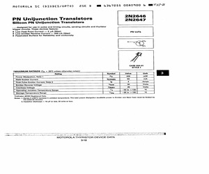
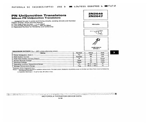
2N2646 2N2647 @ Low Peak Point Current 2 2A (Max) PN UJTs Low Emitter Reverse Current 200 nA (Max) Passivated Surface for Reliability and Uniformity 83 E By fj CASE 22A-01 STYLE 1 *MAXIMUM RATINGS (Ta = 26C unless otherwise noted.) Rating ; . Symbol Value Unit Power Dissipation, Note 1 7 Pp 300 mW RMS Emitter Current lE(RMS) 50 mA Peak Pulse Emitter Current, Note 2 ; ig 2 Amps Emitter Reverse Voltage ; ; Vp2e 30 Volts Interbase Voltage ; Ve2B1 er) Volts Operating Junction Temperature Range a Ty ~65 to +125 Storage Temperature Range Tstg -65 to +150 C Indicates JEDEC Registered Data. Notes: 1. Derate 3 mW/C increase in ambient temperature. The total power dissipation (available power to Emitter and Base-Two} must be limited by the external circuitry. 2, Capacitor discharge 10 yF or less, 30 volts or less. ETO Sa ae ee Fe foe De EES ae MOTOROLA THYRISTOR DEVICE DATA 3-19 MOTOROLA SC (DIODES/OPTO) 2N2646 2N2647 eSE D M@ 6367255 00860901 6 T-37-a/ *ELECTRICAL CHARACTERISTICS (Ta = 25C un
 2 Pages, 127 KB, Scan
2N2646 2N2647 @ Low Peak Point Current 2 A (Max) PN UJTs Low Emitter Reverse Current 200 nA (Max) Passivated Surface for Reliability and Uniformity B2 E By I CASE 22A-01 STYLE 1 *MAXIMUM RATINGS (Ta = 26C unless otherwise noted.) Rating ; . Symbol Value Unit Power Dissipation, Note 1 oe Pp 300. mw RMS Emitter Current le(RMS) 50 mA Peak Pulse Emitter Current, Note 2 . ig 2 Amps Emitter Reverse Voltage - ; Va2E 30 Volts Interbase Voltage ; Ve2B81 35 Volts Operating Junction Temperatura Range i Ty ~66 to +125 Storage Temperature Range Tstg 65 to +150 C Indicates JEDEC Registared Data. Notes: 1. Derate 3 mWPC increase in ambient temperature. Tha total power dissipation (available power to Emitter and Base-Two) must be limited by the external circuitry. 2. Capacitor discharge 10 uF or less, 30 volts or legs. Tea tg z = TERE 2 OIE VTP Beene 2 a a Le MOTOROLA THYRISTOR DEVICE DATA 3-19MOTOROLA SC (DIODES/0OPTO) 25E D 2N2646 @ 2N2647 *ELECTRICAL CHARACTERISTICS (Ta = 25C unless otherwise not
 2 Pages, 70 KB, Scan
20 =MU 10: 2a 10-72 MU 10 28V, 0,05A, Ip<2uA, Iv>2mA, n=0,56...0,75,Rbb>4,7kQ 24c (=1,5x28) 2N4851, 2N4947, 2N4948, 2N4893 =MU 851: [p<2yA, lvo4mA, n20,7...0,85 24c (=1,5x20) 2N4852, 2N4892 =MU 851: Ip<0,4uA, Iv>4mA, 1420,7...0,85 24 (=1,5x28) _ _ - _ ee =2N2646...2647: 7b T0-92 2N2646....47 =2N2646. ..2647: at 10-18 ee _ 2N2646...47 _ ~~ =2N4891: 7b T0-92 2N4891 =2N4892: 7b TO-92 2N4892 =2N4893: 7b TO-92 2N4893 =2N4894; To 0-92 ee 2N4894 co - _ FRr, 50...1000V, 1A, <75ns 3a DO-41 BYV 26B...E _FRr, 50...1000V, 4A, <75ns ___3ia DO-27 a - oe yr, 50...200V, 2x3A, <35ns 17e 10-220 ee YP 20- YO BB. _ _ 47k 0-220 BYT 12P/... P-FR;, 50...600V, 15A, <60ns 17k TO-220 - _ BYT 87. _ Dual, P FRr, 50...600V, 2x8A,<25...50ns Te TO-220 BYV 34... , FE 16A...d ee P FRr, 50...200V, 25, <50ns 82a 00-4 BvW 31/... Dual, P FRr, 50...600V, 30A, <35...60ns 18 STOOP BYV 72/..., BYV 74/..., BYW 99P/... PFRr, 50...200V, 50A, <50ns 32a DO-5 BYWO7/..., BYW78/..., BYW93/..., BYW94/... PF
 1 Pages, 101 KB, Scan
ach can be used for various non-trigger applications. The featuresboth in design and characteristicswhich you receive with these products are concisely defined for each series: TYPES CONVENTIONAL UNIJUNCTIONS 2N489-494proved reliability; MIL spec version. 2N2646-47low cost, proved hermetic sealed device. PROGRAMMABLE UNIJUNCTION TRANSISTOR (PUT)variable threshold, low cost, fast switching speed, and circuit adjustable electrical characteristics. COMPLEMENTARY UNIJUNCTION TRANSISTORu!timate in temperature stability for timing and oscillator applications. SILICON UNILATERAL SWITCH (SUS)-a stable fixed low voltage threshold, low cost, high performance 4-layer diode. SILICON BILATERAL SWITCH (SBS)low voltage triac trigger, two silicon unilateral switches connected back to back. SILICON CONTROLLED SWITCH (SCS)high triggering sensitivity, 4-lead capability for multiple loads or dv/dt suppression. APPLICATIONS Unijunctions . Device Triggers Conventional Complementary Programmable 2N489-94, 2N2646<
 6 Pages, 887 KB, Scan
1845 2N 1846 2N1847 2N1848 2N1849 2N1850 2N1909 2N1910 2N1911 Type 2N1912 2N1913 2N1914 2N1915 2N1916 2N2023 2N2024 2N2025 2N2026 2N2027 2N2028 2N2029 2N2030 2N2160 2N2322 2N2323 2N2324 2N2325 2N2326 2N2327 2N2328 2N2329 2N2344 2N2345 2N2346 2N2347 2N2348 2N2646 2N2647 2N2840 2N3870 2N3871 2N3872 2N3873 2N3877 2N3896 2N3897 2N3898 2N3899 2N3903 2N3904 2N3905 2N3906 2N4123 2N4124 2N4125 2N4126 2N4400 2N4401 2N4402 2N4403 2N4409 2N4410 2N4983 2N4984 2N4985 2N4986 2N4987 2N4988 2N4989 2N4990 2N4991 2N4992 2N4993 2N5060 2N5061 2N5062 2N5063 2N5064 2N5088 2N5089 2N5174 2N5175 2N5176 2N5204 2N5205 2N5206 2N5207 2N5219 2N5220 2N5221 2N5223 2N5225 2N5226 2N5227 2N5305 2N5306 2N5307 2N5308 2N5777 2N5778 2N5779 2N5780 2N6027 2N6028 3N81 3N82 3N83 3N84 3N85 3N86 4N25 4N26 4N27 4N28 4N29 4N30 4N31 4N32 4N33 4N35 4N36 4N37 4N38 4N39 4N40 Al4a* A15* A2B8* A40* A44* A7O* A1l14* A115 A139* A170* Al77 A180 A1g87* A190* A197* A390 A397* A430* A437* A500* A540* A5S70* AS96* A640 A696 * BCc* BD* BPW* c3* c5* C6" cr
 91 Pages, 27912 KB, Scan
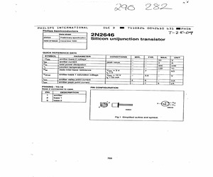
2N2646 th ops an . J ee __[Protninary sects"! Silicon unijunction transistor date of issue | December 1990 QUICK REFERENCE DATA SYMBOL PARAMETER CONDITIONS MIN. TYP. MAX, UNIT Vege amitter-base 2 voltage - - 30 v leg emitter current peak value - - 2 A Pr total power dissipation - - 300 mW Ty, Junction temperature - ~ 125 C Pog Static inter-base resistance Vee) = 3 V - 7 - kQ =O Veptent emitter-base 1 saturation voltage Viet = 10V - 3.5 - v I, =50 mA lean emitter valley point current 4 6 - mA ew) emitter peak point current - 1 5 pA PINNING - TO-18 PIN CONFIGURATION Base 2 connected to case. PIN DESCRIPTION emitter 2 jbase1 3 | base2 wy | SS by 3 MBBISS MSB031 Fig.1 Simplified outline and symbol. 733Philips Semiconductors ew Silicon unfjunction transistor SKE D MM 7110826 004261) 578 MMPHIN ene ee PHILIPS INTERNATIONAL Preliminary specification 2N2646 LIMITING VALUES T- 25-09 In accordance with the Absolute Maximum System (IEC 134). SYMBOL PARAMETER CONDITIONS MIN, MAX. UNIT ~Vepe amit
 4 Pages, 132 KB, Scan
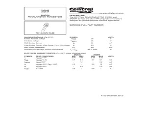
2N2646 2N2647 SILICON PN UNIJUNCTION TRANSISTORS w w w. c e n t r a l s e m i . c o m DESCRIPTION: The CENTRAL SEMICONDUCTOR 2N2646 and 2N2647 devices are silicon PN Unijunction Transistors designed for general purpose industrial applications. MARKING: FULL PART NUMBER TO-18 (UJT) CASE MAXIMUM RATINGS: (TA=25C) Emitter Reverse Voltage Interbase Voltage RMS Emitter Current Peak Emitter Current (Duty Cycle 1%, PRR10pps) RMS Power Dissipation Operating and Storage Junction Temperature SYMBOL VB2E VB2B1 VB2E=30V IV IP VB2B1=20V, RB2=100 VB2B1=25V VOB1 V1=20V UNITS V 35 V Ie ie 50 mA 2.0 A PD TJ, Tstg 300 mW -65 to +150 C ELECTRICAL CHARACTERISTICS: (TA=25C unless otherwise noted) 2N2646 SYMBOL TEST CONDITIONS MIN MAX VB2B1=10V 0.56 0.75 RBB VB2B1=3.0V 4.7 9.1 IEB2O 30 2N2647 MIN MAX 0.68 0.82 UNITS 4.7 9.1 k 12 - 0.2 A 4.0 - 8.0 18 mA - 5.0 - 2.0 A 3.0 - 6.0 - V - R1 (2-December 2013) 2N2646 2N2647 SILICON PN UNIJUNCTION TRANSISTORS TO-18 (UJT) CASE - MECHANICAL
 4 Pages, 734 KB, Original


